
High Frequency PCB Traces
High frequency PCB traces behave like transmission lines, with a precise impedance value at every point along their length. If the impedance changes, a reflected signal will be generated that can interfere with the original waveform and significantly degrade its quality. Impedance control is an essential design requirement for high-frequency signals, whether they are differential pair (LVDS), single-ended, or RF.
The characteristic impedance of a transmission line is its resistance, capacitance and inductance expressed as a combination of ohms. The value of this impedance is typically 50 ohms for most standard digital and analog signals, but can vary depending on the signaling protocol used in the device.
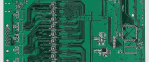
There are a number of factors that influence the impedance of a PCB trace, and many of them are easy to control in the design stage. The width of the trace, copper thickness and the dielectric constant of the substrate are all important to consider when designing a high frequency pcb.
Impedance Values for High Frequency PCB Traces
In order to achieve the required impedance, it is often necessary to change one or more of these factors. For example, changing the thickness of the insulating layer can make a significant difference to the impedance. A 0.025mm increase in laminate thickness can cause an impedance change between 5 and 8 ohms, so it is vital to carefully select this parameter during the design process.
Another factor that influences the impedance of a PCB is the trace spacing between different signals. In general, it is best to route differential pairs of signal traces parallel to each other. This will help to reduce interference between them, and maintain symmetry. In addition, it is often a good idea to follow the 3W or 2W rules, which will ensure that there is adequate spacing between controlled impedance traces, and other traces and components on the circuit board.
If you are designing a high-frequency PCB, the component datasheet will often provide comprehensive information on which signals require impedance management, including recommended trace widths and copper weights. Following these guidelines will help to ensure that your PCB is built with the correct impedance for the specific application.
In addition to the above tips, it is also important to carefully specify which signals need impedance control during the design stage. Specifying this in the documentation that is sent to the PCB fabricator can help them to understand your specific requirements, and avoid making any mistakes during production.
This will save you time and money in the long run. For more detailed information on how to specify these parameters, you can visit the Sierra Circuits blog for a detailed article on the subject. Then, you can get started on your next high-speed project with confidence. Contact us to discuss your requirements or to request a quote today. We look forward to hearing from you!.
