
Integrity of PCB Design & Assembly With DFT Techniques
The integrity of a printed circuit board (PCB) is an essential factor from both a technical and financial perspective. Product failures can result in costly recalls, repairs, and replacements, while a loss of customer trust can damage a brand’s reputation and market position. For safety-critical applications, such as in medical devices or automotive electronics, rigorous testing is even more important. The good news is that PCB manufacturers can minimize the chances of faulty products by designing their PCBs with testability in mind. This is accomplished by using design for testability (DFT) techniques.
As the demand for high-speed, performance-driven, yet miniature electronic devices continues to rise, it becomes increasingly challenging for manufacturers to keep up with consumers’ ever-changing expectations. These new demands call for higher-frequency signals, smaller components, buried or blind vias, and more layers in a PCB. As a result, manufacturers must use sophisticated inspection and testing techniques to ensure the integrity of their final products.
Luckily, there are several techniques available to help manufacturers confirm the integrity of a pcb design & assembly before it’s manufactured. The first step in achieving this goal is to have a robust design that’s manufacturable, which can be verified through functional testing. Functional testing involves simulating electrical signals capable of stimulating the circuit and observing the results, which can be used to verify that the circuit meets its original design requirements.
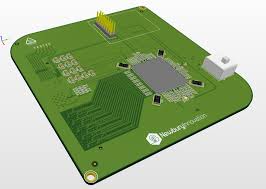
Test the Integrity of PCB Design & Assembly With DFT Techniques
Another key factor that can be tested with bare-board testing is signal integrity, which can be determined by measuring the resistance between electrical connections and checking for shorts and open circuits. Performing this type of testing helps to ensure that the circuit’s high-speed connections are not negatively impacted by other elements in the PCB, such as impedance mismatches or discontinuities in the routing topology.
Finally, a comprehensive test plan should also include inspections of the solder joints and the component packages, which can be verified with a bed of nails tester or flying probe tester. In addition to these bare-board tests, an in-circuit test (ICT) can be performed on the assembled PCB to detect problems such as missing or damaged components, improper grounding, and misplaced or broken connections. This test can be conducted with specialized ICT equipment, which can also check for a number of other issues like component placement and positioning.
A partnership with an experienced ECM will be vital to ensuring that your prototypes are properly tested and ready for manufacturing. They will know which testing methods are best suited to your specific needs, and will be able to guide you on how to optimize your PCB design for better testing results. To make the most of this partnership, you should communicate with your ECM frequently, and consult them on your design choices to ensure that your PCB is ready for production. This will help you reduce the cost of your test program and increase your chances of launching a high-quality, reliable product.


